Capabilities
One PCB partner. Full-spectrum capability.
From single-sided prototypes to 50-layer high-density boards, Sunrise has the equipment, process control and engineering support to handle your toughest builds.
Quick-Turn Prototype & Production
Prototype completion in just 12 hours — the new industry standard. Agile responses to evolving market demands.
15:1 Drill Aspect Ratio
Precision techniques delivering unparalleled accuracy in our drilling processes for the most demanding requirements.
2 – 50 Layer Multilayers
Double-sided, multilayer, and the most complex/complicated designs handled in-house with consistent quality.
Maximum Panel Size 24" × 30"
Custom panel sizes accommodate dimensions up to 24×30 inches — a precise fit for unique applications.
High Volume Capabilities
Strategic high-volume production and supply-chain management for optimal efficiency and customer satisfaction.
Advanced Vias
Blind & buried vias (BBVs), micro vias, and via-in-pad with multiple fill options including conductive and non-conductive.
Fine Line & Spacing
Down to 3 mil trace and space for high-density interconnect (HDI) designs and modern miniaturized layouts.
Controlled Impedance
Tight tolerance impedance control ±5% for high-speed signal integrity in RF and digital designs.
IPC Class 2 / 3
Manufacturing to IPC-A-600 Class 2 and Class 3 standards including military and medical applications.
Rigid-Flex & Flex
Rigid-flex, flex circuits and rigid-flex with HDI — including mixed-dielectric (hybrid) and copper-core constructions.
Embedded Passives
Buried capacitance and buried resistor technology for noise reduction, miniaturization and improved signal integrity.
Advanced Microvias
Pico/CO₂ laser drilling, stacked, staggered, stacked-on-buried and variable-depth microvias down to 2 mil.
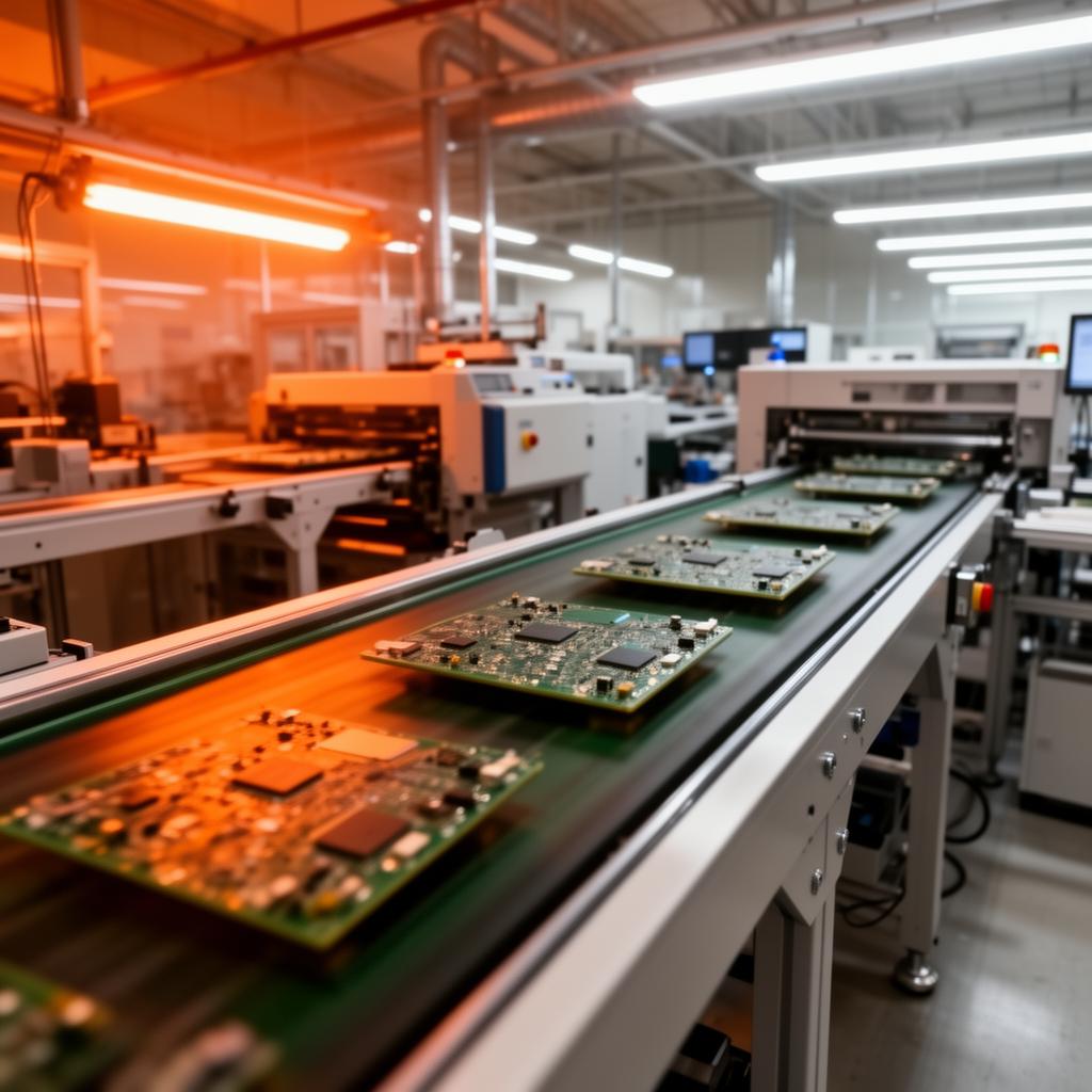
In-house production
From bare laminate to finished board — under one roof.
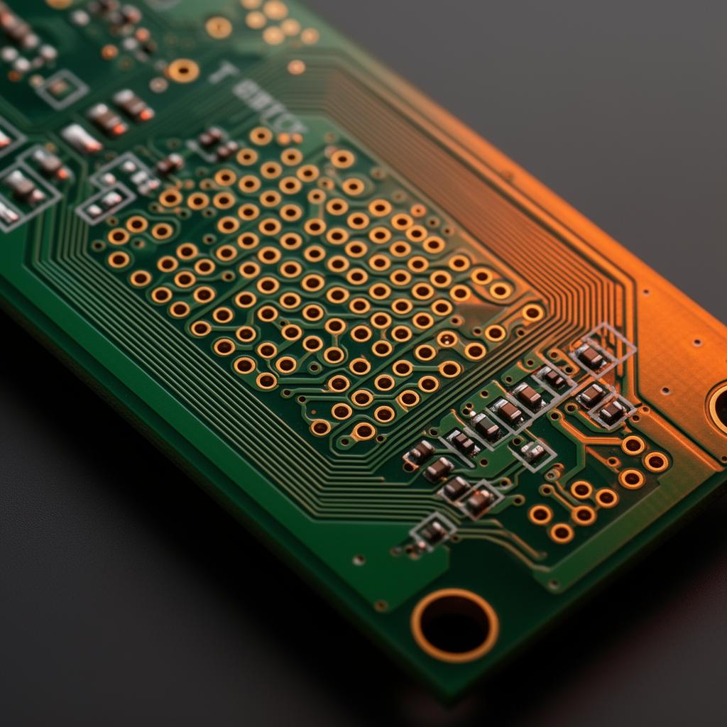
Multilayer · 2–50 layers
HDI · Microvia
Capability Matrix
The numbers that matter.
| Layer count | 2 – 50 layers |
| Min trace / space | 1 mil / 1 mil |
| Min hole size | 6 mil mechanical · 3 mil laser |
| Drill aspect ratio | Up to 15:1 |
| Max panel size | 24" × 30" |
| Max board thickness | 0.250" |
| Min board thickness | 0.008" |
| Copper weight | 0.5 oz – 10 oz |
| Surface finishes | ENIG, HASL, LF-HASL, OSP, Immersion Ag/Sn, Hard Gold |
| Solder mask | LPI — Green, Black, Red, Blue, White, Yellow, Matte |
| Lead time | Same day, 24h, 48h, 5-day standard |
| Standards | IPC-A-600 Class 2 & 3, UL, RoHS, ITAR-aware |
Process Tiers
Standard, Medium, Advanced & Development.
Our in-house capability scales across four process tiers — from production-friendly Standard work to leading-edge Development specs for the most aggressive designs.
General
| Parameter | Standard | Medium | Advanced | Development |
|---|---|---|---|---|
| Maximum board thickness | .125" | .250" | .250" | .300" |
| Minimum board thickness | .005" | .004" | .002" | .002" |
| Board thickness tolerance | ±10% | ±7% | ±5% | ±5% |
| Maximum layer count | 20 layer | 30 layer | 50 layer | 60+ layer |
| Maximum bow & twist | 10% | 10% | 10% | 5% |
| Minimum core thickness | .002" | .002" | .002" | .002" |
| Minimum prepreg thickness | .0016" | .0016" | .0016" | .001" |
| Layer registration tolerance | .005" | .005" | .003" | .003" |
| Min. epoxy-filled via | .008" | .006" | .004" | .004" |
| Max. epoxy-filled via | .014" | .016" | .020" | .020" |
| Min. copper-filled via | .008" | .006" | .003" | .002" |
| Max. copper-filled via | .012" | .014" | .014" | .014" |
Line Width / Space — Non-plated
| Parameter | Standard | Medium | Advanced | Development |
|---|---|---|---|---|
| 3/8 oz copper | .003" | .002" | .001" | — |
| 0.5 oz copper | .003" | .002" | .001" | — |
| 1 oz copper | .003" | .003" | .002" | .001" |
| 2 oz copper | .005" | .004" | .004" | .003" |
| 3 oz copper | .007" | .006" | .005" | .004" |
| 4 oz copper | .012" | .010" | .008" | .006" |
Line Width / Space — Plated (I/L = O/L)
| Parameter | Standard | Medium | Advanced | Development |
|---|---|---|---|---|
| 3/8 oz + plating | .003" | .002" | .001" | — |
| 0.5 oz + plating | .003" | .002" | .001" | — |
| 1 oz + plating | .003" | .003" | .002" | .001" |
| 2 oz + plating | .004" | .003" | .002" | .001" |
Solder Mask
| Parameter | Standard | Medium | Advanced | Development |
|---|---|---|---|---|
| Min SMD mask web | .005" | .004" | .003" | .002" |
| Min SMD mask opening | .005" | .004" | .003" | .002" |
| Min PTH mask opening | .006" | .005" | .004" | .002" |
| Registration tolerance | .003" | .003" | .002" | .001" |
Impedance Control
| Parameter | Standard | Medium | Advanced | Development |
|---|---|---|---|---|
| Single-ended tolerance | ±10% | ±5% | ±5% | ±2% |
| Broadside differential | ±10% | ±5% | ±5% | ±2% |
| Edge-coupled differential | ±10% | ±5% | ±5% | ±2% |
Detailed Specifications
Drilling, microvia, finishes & profile.
Mechanical Drill
- Min drilled via — < .062" board
- .008"
- Min drilled via — .062" board
- .008"
- Min drilled via — .093" board
- .008"
- Min drilled via — .125" board
- .010"
- Min drilled via — .187" board
- .016"
- Min drilled via — > .187" board
- .018"
- Max drill hole size
- .250"
- Min hole positional tolerance
- .003"
- Min hole-to-hole (same layer)
- .008"
- Min hole-to-hole (different layers)
- .008"
- Back-drill stub length
- .005"
- IL pad over drill (0.001" annular ring)
- .008"
- OL pad over drill (0.002" annular ring)
- .010"
- Maximum aspect ratio (drilled through)
- 10:1
- Press-fit hole tolerance
- .002"
- Cu-filled mech. drilled — max drill
- .012"
- Cu-filled mech. drilled — max aspect ratio
- 10:1
Laser Drill / Microvia
- Min microvia size
- .002"
- Max microvia size
- .012"
- Capture pad size (Class 3)
- .006"
- Maximum aspect ratio
- 1:1
- Min via-to-via (same layer)
- .008"
- Min via-to-via (staggered, different layers)
- .008"
- Min laser via to mechanical via
- .008"
- Laser equipment
- Pico / CO₂
- Through-via uvia size
- .008"
- Variable-depth uvia size
- .005"
In-house Surface Finishes
- ENIG
- In-house · 2–3 µin
- ENEPIG
- In-house · 2–11 µin
- Gold over nickel
- In-house · 2–50 / 50–100 / up to 200 µin
- Hard gold edge connectors
- In-house · 2–50 / 50–100 / up to 200 µin
- Selective gold (flash + Imm Ag)
- In-house
- Selective gold (flash + H-gold)
- In-house
- LF-HASL
- On-site
- Immersion Silver / Tin / OSP / HASL
- Available (outside service)
- Combination finishes
- Gold/LF-HAL · OSP/ENIG · Tin/Gold · ENEPIG/ENIG
Outline Profile & V-Cut
- Standard router bit sizes
- .031 / .040 / .050 / .062 / .093 / .100"
- Min internal rout radius
- .015"
- Min routed slot width
- .012"
- Min copper-to-edge clearance
- .010"
- Min hole edge to board edge
- .012"
- Edge milling
- Available
- Jump scoring
- Available
- V-cut top/bottom alignment
- .003"
- V-cut residual thickness tolerance
- .015"
- V-cut available angles
- 20° / 30°
Specialty Capabilities
Beyond the standard process flow.
Cavity, embedded passive, hybrid and high-density technologies — all available in-house under one roof.
Don't see a spec listed? We probably do it.
Talk to our engineering team about custom requirements.